6. Semiconductors
Definitions
- Transistors are low impedance, current operated devices
- Thermal Runaway is self destruction of the transistor when the the current passing through a transistor increases, heat is generated
- Depletion layer is an area depleted of mobile electrons (or holes) for carrying current
- Ohmic region is the steep part of the curve and it is similar to resistance
Diagrams
-
Forward bias and reverse bias
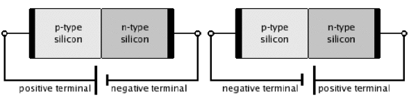
Image credit: Academics easy
-
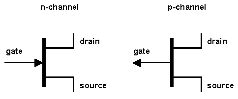
Field Effect Transistors (source +, drain -)

Image credit: Wikipedia
Circuit Symbols
-
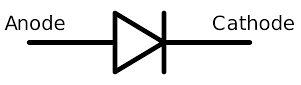
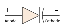
Diode
-
Zener Diode
-
Variable capacitor diode
-
Transistors with emitter, base and collector

-
Field Effect Transistors
Circuits
-
FET Amplifier

Image credit: Electronics Tutorials
-
Common Emitter, Common Base, Common Collector
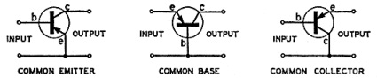
Image credit: Vintage radio
Graphs
-
Diode graph
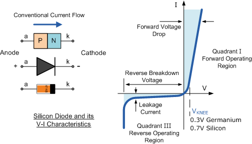
Image credit: Electronics Tutorials
-
FET Graphs
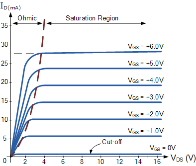
Image credit: Electronics stackexchange
Notes
P-type and N-type
- Germanium has four electrons in its outer orbit
- 4 valence electrons are used in current flow
- Pure Germanium does not conduct electricity
- if a minute quantity of a certain impurity is added, its resistance is greatly reduced
| N-type | P-type | |
|---|---|---|
| Impurity | Arsenic | Indium |
| Valency | 5 | 3 |
| Name | N-type: mobility of electrons | P-type: mobility of a missing electron (hole) |
| Condition | an excess of electrons | an excess of holes |
Forward and reverse biased
| Forward bias | Reverse bias |
|---|---|
(+) terminal of battery is connected to p-type (-) terminal of battery is connected to n-type |
(+) terminal of battery is connected to n-type (-) terminal of battery is connected to p-type |
| depletion layer is very thin | depletion layer is very thick |
| p-n junction offers low resistance | p-n junction offers high resistance |
| ideal diode have zero resistance | ideal diode has infinite resistance |
| current will flow | no current will flow |
| low impedance | high impedance |
Diode
- Current flows when the voltage is positive
- Virtually no current flows when the voltage is negative
- Forward part of the characteristic is not linear
- Small positive voltage is needed for current flow
0.3Vfor Germanium0.7Vfor Silicon (more pd. is needed as there are lesser atom shells to remove the valence electron for current flow)
- Reverse (-V) direction just a few
µAflows unless the breakdown voltage is exceeded
Zener diode
- Reverse characteristic can be designed to pass a considerable current
- Pre-designed critical voltage
- Application: voltage stabilizer circuits
Variable capacitance diode
- self capacitance of a diode varies as the voltage is changed
- reverse characteristic can be designed so that this change in capacitance can be used
- Application: electronic tuning circuits
Bipolar Junction Transistor
- PNP (usually Germanium) and NPN (usually Silicon)
- 3 currents at Emitter, Base and Collector are interdependent
- Input and output current are almost the same
- Large difference between the input and output impedances that is the key to transistor amplification because
P = I²R - There is no direct connection between Emitter and Collector
Transistor operation
| NPN / PNP | Common base |
Common emitter |
Common collector* |
|---|---|---|---|
| Current gain | < 1 | 49 | 50 |
| Power gain | 1000 | 1000 | < 1 |
| Input impedance | Low | Med | Hi |
| Output impedance | Hi | Med | Lo |
* Common collector == emitter follower
For practical transistor biasing, the base should be
0.3vmore negative than the emitter, for a PNP Germanium transistor0.3vmore positive than the emitter, for NPN Germanium transistor0.7vmore positive than the emitter, for NPN Silicon transistor0.7vmore negative than the emitter, for PNP Silicon transistor
Thermal runway
- Precaution:
- a resistor in the emitter lead
- will act in opposition to base bias and reduce current
- by-pass (decoupling) capacitor is usually connected across the emitter resistor
- to avoid a reduction of the A by-wanted AC signal
- a resistor in the emitter lead
Field Effect Transistor
- Connections are made to each end of the N type channel material
- Small negative Gate voltage:
- creates a small depletion area
- current carrying channel is slightly restricted
- medium negative Gate voltage:
- creates a medium depletion area
- current carrying channel is further reduced
- higher negative Gate voltage
- makes the depletion areas meet in the middle
- completely blocks the channel, cutting off the current flowing from Drain to Source
FET Amplifier
- Source resistor is by-passed with a large capacitor to prevent a reduction in the wanted AC Signal
- The input impedance will be very high; the same value of the gate resistor
- The output impedance will equal the Drain load resistor
- !! Take care to not build up static electricity: don’t wear nylon t-shirt while soldering
- Precaution: It has high impedance
Integrated circuits
- E.g. Transistors, amplifiers, mixers, radio receivers
- Made of Silicon and are connected to the PCB via legs / pins
- Not applicable: Speaker, variable capacitor, coils